- 您现在的位置:买卖IC网 > Sheet目录1991 > CS4398-CZZ (Cirrus Logic Inc)IC DAC 120DB 192KHZ W/VC 28TSSOP
16
DS568F1
CS4398
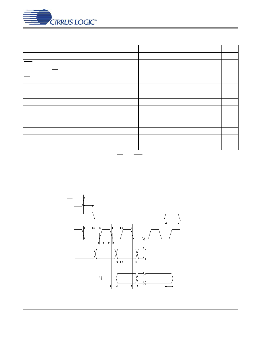
SWITCHING CHARACTERISTICS - CONTROL PORT - SPI FORMAT
(Inputs: Logic 0 = GND, Logic 1 = VLC, CL =20pF)
11. tspi only needed before first falling edge of CS after RST rising edge. tspi = 0 at all other times.
12. Data must be held for sufficient time to bridge the transition time of CCLK.
13. For FSCK < 1 MHz.
14. CDOUT should not be sampled during this time period.
15. This time is by design and not tested.
Parameter
Symbol
Min
Max
Unit
CCLK Clock Frequency
fsclk
-6
MHz
RST Rising Edge to CS Falling
tsrs
500
-
ns
CCLK Edge to CS Falling
(Note 11)
tspi
500
-
ns
CS High Time Between Transmissions
tcsh
1.0
-
s
CS Falling to CCLK Edge
tcss
20
-
ns
CCLK Low Time
tscl
66
-
ns
CCLK High Time
tsch
66
-
ns
CDIN to CCLK Rising Setup Time
tdsu
40
-
ns
CCLK Rising to DATA Hold Time
(Note 12)
tdh
15
-
ns
Rise Time of CCLK and CDIN
(Note 13)
tr2
-100
ns
Fall Time of CCLK and CDIN
(Note 13)
tf2
-100
ns
Transition time from CCLK to CDOUT valid
tscdov
-40
ns
Time from CS rising to CDOUT high-Z
tcscdo
-20
ns
t
r2
t
f2
t dsu t dh
t
sch
t scl
CS
CCL K
CD IN
t css
t
csh
t spi
t srs
RST
CD O UT
t
scdov
t
sc do v
t cscdo
Hi-Im pedance
Figure 9. Control Port Timing - SPI Format (Read/Write)
发布紧急采购,3分钟左右您将得到回复。
相关PDF资料
CS43L22-CNZR
IC DAC W/HDPN & SPKR AMPS 40-QFN
CS4461-CZZR
IC ADC PSR FEEDBACK 24-TSSOP
CS5340-CZZ
IC ADC AUD 101DB 200KHZ 16-TSSOP
CS5340-DZZR
IC ADC AUD 101DB 200KHZ 16-TSSOP
CS5341-DZZ
IC ADC AUD 105DB 200KHZ 16-TSSOP
CS5342-CZZ
IC ADC AUD 105DB 200KHZ 16-TSSOP
CS5345-CQZ
IC ADC AUD 104DB 200KHZ 48-LQFP
CS5345-DQZ
IC ADC AUD 104DB 200KHZ 48-LQFP
相关代理商/技术参数
CS4398-CZZR
功能描述:数模转换器- DAC IC 120dB 192kHz Mlt-Bt DAC w/Volctrl RoHS:否 制造商:Texas Instruments 转换器数量:1 DAC 输出端数量:1 转换速率:2 MSPs 分辨率:16 bit 接口类型:QSPI, SPI, Serial (3-Wire, Microwire) 稳定时间:1 us 最大工作温度:+ 85 C 安装风格:SMD/SMT 封装 / 箱体:SOIC-14 封装:Tube
CS4399-CNZ
功能描述:HIPRFDACINTGHPDRIVR&IMPED DETCTN 制造商:cirrus logic inc. 系列:* 包装:托盘 零件状态:在售 安装类型:表面贴装 封装/外壳:40-WFQFN 裸露焊盘 供应商器件封装:40-QFN(5x5) 标准包装:490
CS4399-CNZR
功能描述:HIPRFDACINTGHPDRIVR&IMPED DETCTN 制造商:cirrus logic inc. 系列:* 包装:剪切带(CT) 零件状态:在售 安装类型:表面贴装 封装/外壳:40-WFQFN 裸露焊盘 供应商器件封装:40-QFN(5x5) 标准包装:1
CS4399-CWZR
功能描述:HIPRFDACINTGHPDRIVR&IMPED DETCTN 制造商:cirrus logic inc. 系列:* 包装:剪切带(CT) 零件状态:在售 安装类型:表面贴装 封装/外壳:42-UFBGA,WLCSP 供应商器件封装:42-WLCSP 标准包装:1
CS43L21
制造商:CIRRUS 制造商全称:Cirrus Logic 功能描述:Low Power, Stereo Digital to Analog Converter
CS43L21-CNZ
功能描述:音频数/模转换器 IC Low Power Stereo DAC 24-Bits 96kHz 98dB RoHS:否 制造商:Texas Instruments 转换器数量: 分辨率:16 bit 接口类型:I2S, UBS 转换速率: 信噪比:98 dB 工作电源电压:5 V DAC 输出端数量:2 工作温度范围:- 25 C to + 85 C 电源电流:23 mA 安装风格:SMD/SMT 封装 / 箱体:TQFP-32 封装:Reel
CS43L21-CNZR
功能描述:数模转换器- DAC IC 98dB 96kHz Low PWR Stereo DAC RoHS:否 制造商:Texas Instruments 转换器数量:1 DAC 输出端数量:1 转换速率:2 MSPs 分辨率:16 bit 接口类型:QSPI, SPI, Serial (3-Wire, Microwire) 稳定时间:1 us 最大工作温度:+ 85 C 安装风格:SMD/SMT 封装 / 箱体:SOIC-14 封装:Tube
CS43L21-DNZ
功能描述:数模转换器- DAC CS43L21-DNZ MS Audio Portable part. RoHS:否 制造商:Texas Instruments 转换器数量:1 DAC 输出端数量:1 转换速率:2 MSPs 分辨率:16 bit 接口类型:QSPI, SPI, Serial (3-Wire, Microwire) 稳定时间:1 us 最大工作温度:+ 85 C 安装风格:SMD/SMT 封装 / 箱体:SOIC-14 封装:Tube